
Stock Code
301678

HENGHUI provides customers with one-stop packaging solutions, covering the entire process from wafer BG and sawing, packaging, FT testing, to IoT card personalization. The company has its own high-speed tin-plating line, and the packaging workshop is certified under the IATF16949 Quality Management System, with a monthly capacity of 35 million units. Main product series include DFN, QFN, and MP2, with a focus on etched leadframe packaging, committed to providing customers with high-reliability products and first-class services.
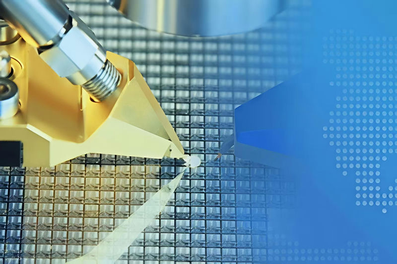
Wafer Diameter (BG, Sawing, Die Bonding): : 6 inches, 8 inches, 12 inches
Minimum BG Thickness: 100μm
Minimum Dicing Saw Slot Width (Blade): 60μm
Process: LOW - K/Non - LOW - K
Minimum Dicing Saw Slot Width (Laser): :60μm
Minimum Chip Size (Die): 0.15*0.15mm
Minimum Bonding Pad Pitch (BPP, Gold Wire): 45μm
Minimum Bonding Pad Open (BPO, Gold Wire): 40*40μm²
Minimum Bonding Pad Pitch (BPP, Alloy Wire): 50μm
Minimum Bonding Pad Open (BPO, Gold Wire): 43*43μm
Minimum Bonding Pad Pitch (BPP, Gold Wire, Alloy Wire, Gold Wire): 55μm
Minimum Bonding Pad Size (BPO, Gold Wire, Alloy Wire, Gold Wire): 45*45μm
Wire Diameter: 15-50μm
Wire Length: 0.2-4mm
Al thickness on Pad (Gold Wire): Al-Cu structure ≥0.6μm
Al thickness on Pad (Alloy Wire): Al-Cu/Al-Si-Cu structure ≥0.8μm
Al thickness on Pad (Gold Wire, Alloy Wire, Gold Wire): Al-Cu/Al-Si-Cu structure ≥1.2μm
Previous: QFN Module
Next: New MP2 Packaging